Engineers are available to assist.

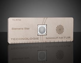
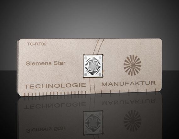
High Resolution Microscopy Star Target, #37-538
High Resolution Microscopy Slide Targets are designed using high-precision e-beam lithography. The patterns are etched on a 10 × 10mm² fused silica substrate with broad spectral transmission (DUV-VIS-NIR), on which a chromium layer of high optical density is applied. By removing the chromium layer, patterns are created in sizes down to 100nm. High Resolution Microscopy Slide Targets provide excellent dimensional stability and are mounted in a metal microscope slide holder. The negative patterns on each target allow the structures to be transparent, while the background is blocked by a chrome layer.


or view regional numbers
QUOTE TOOL
enter stock numbers to begin
Copyright 2025 | Edmund Optics BV, De Maas 22B, 5684 PL Best, The Netherlands
California Consumer Privacy Acts (CCPA): Do Not Sell or Share My Personal Information
California Transparency in Supply Chains Act
The FUTURE Depends On Optics®