


Imaging Electronics 101: Understanding Camera Sensors for Machine Vision Applications
Construction | Features | Spectral Properties
Imaging electronics, in addition to imaging optics, play a significant role in the performance of an imaging system. Proper integration of all components, including camera, capture board, software, and cables results in optimal system performance. Before delving into any additional topics, it is important to understand the camera sensor and key concepts and terminology associated with it.
The heart of any camera is the sensor; modern sensors are solid-state electronic devices containing up to millions of discrete photodetector sites called pixels. Although there are many camera manufacturers, the majority of sensors are produced by only a handful of companies. Still, two cameras with the same sensor can have very different performance and properties due to the design of the interface electronics. In the past, cameras used phototubes such as Vidicons and Plumbicons as image sensors. Though they are no longer used, their mark on nomenclature associated with sensor size and format remains to this day. Today, almost all sensors in machine vision fall into one of two categories: Charge-Coupled Device (CCD) and Complementary Metal Oxide Semiconductor (CMOS) imagers.
Sensor Construction
Charge-Coupled Device (CCD)
The charge-coupled device (CCD) was invented in 1969 by scientists at Bell Labs in New Jersey, USA. For years, it was the prevalent technology for capturing images, from digital astrophotography to machine vision inspection. The CCD sensor is a silicon chip that contains an array of photosensitive sites (Figure 1). The term charge-coupled device actually refers to the method by which charge packets are moved around on the chip from the photosites to readout, a shift register, akin to the notion of a bucket brigade. Clock pulses create potential wells to move charge packets around on the chip, before being converted to a voltage by a capacitor. The CCD sensor is itself an analog device, but the output is immediately converted to a digital signal by means of an analog-to-digital converter (ADC) in digital cameras, either on or off chip. In analog cameras, the voltage from each site is read out in a particular sequence, with synchronization pulses added at some point in the signal chain for reconstruction of the image.
The charge packets are limited to the speed at which they can be transferred, so the charge transfer is responsible for the main CCD drawback of speed, but also leads to the high sensitivity and pixel-to-pixel consistency of the CCD. Since each charge packet sees the same voltage conversion, the CCD is very uniform across its photosensitive sites. The charge transfer also leads to the phenomenon of blooming, wherein charge from one photosensitive site spills over to neighboring sites due to a finite well depth or charge capacity, placing an upper limit on the useful dynamic range of the sensor. This phenomenon manifests itself as the smearing out of bright spots in images from CCD cameras.
To compensate for the low well depth in the CCD, microlenses are used to increase the fill factor, or effective photosensitive area, to compensate for the space on the chip taken up by the charge-coupled shift registers. This improves the efficiency of the pixels, but increases the angular sensitivity for incoming light rays, requiring that they hit the sensor near normal incidence for efficient collection.
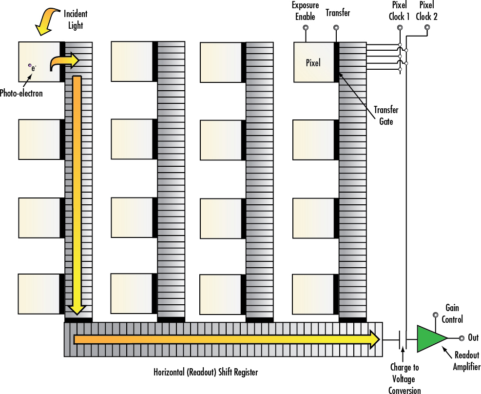
Figure 1: Block Diagram of a Charge-Coupled Device (CCD)
Complementary Metal Oxide Semiconductor (CMOS)
The complementary metal oxide semiconductor (CMOS) was invented in 1963 by Frank Wanlass. However, he did not receive a patent for it until 1967, and it did not become widely used for imaging applications until the 1990s. In a CMOS sensor, the charge from the photosensitive pixel is converted to a voltage at the pixel site and the signal is multiplexed by row and column to multiple on chip digital-to-analog converters (DACs). Inherent to its design, CMOS is a digital device. Each site is essentially a photodiode and three transistors, performing the functions of resetting or activating the pixel, amplification and charge conversion, and selection or multiplexing (Figure 2). This leads to the high speed of CMOS sensors, but also low sensitivity as well as high fixed-pattern noise due to fabrication inconsistencies in the multiple charge to voltage conversion circuits.
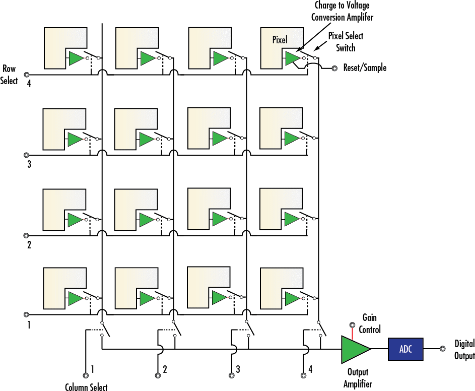
Figure 2: Block Diagram of a Complementary Metal Oxide Semiconductor (CMOS)
The multiplexing configuration of a CMOS sensor is often coupled with an electronic rolling shutter; although, with additional transistors at the pixel site, a global shutter can be accomplished wherein all pixels are exposed simultaneously and then readout sequentially. An additional advantage of a CMOS sensor is its low power consumption and dissipation compared to an equivalent CCD sensor, due to less flow of charge, or current. Also, the CMOS sensor’s ability to handle high light levels without blooming allows for its use in special high dynamic range cameras, even capable of imaging welding seams or light filaments. CMOS cameras also tend to be smaller than their digital CCD counterparts, as digital CCD cameras require additional off-chip ADC circuitry.
The multilayer MOS fabrication process of a CMOS sensor does not allow for the use of microlenses on the chip, thereby decreasing the effective collection efficiency or fill factor of the sensor in comparison with a CCD equivalent. This low efficiency combined with pixel-to-pixel inconsistency contributes to a lower signal-to-noise ratio and lower overall image quality than CCD sensors. Refer to Table 1 for a general comparison of CCD and CMOS sensors.
| Table 1: Comparison of (CCD) and (CMOS) Sensors | ||
|---|---|---|
| Sensor | CCD | CMOS |
| Pixel Signal | Electron Packet | Voltage |
| Chip Signal | Analog | Digital |
| Fill Factor | High | Moderate |
| Responsivity | Moderate | Moderate – High |
| Noise Level | Low | Moderate – High |
| Dynamic Range | High | Moderate |
| Uniformity | High | Low |
| Resolution | Low – High | Low – High |
| Speed | Moderate - High | High |
| Power Consumption | Moderate – High | Low |
| Complexity | Low | Moderate |
| Cost | Moderate | Moderate |
Alternative Sensor Materials
Short-wave infrared (SWIR) is an emerging technology in imaging. It is typically defined as light in the 0.9 – 1.7μm wavelength range, but can also be classified from 0.7 – 2.5μm. Using SWIR wavelengths allows for the imaging of density variations, as well as through obstructions such as fog. However, a normal CCD and CMOS image is not sensitive enough in the infrared to be useful. As such, special indium gallium arsenide (InGaAs) sensors are used. The InGaAs material has a band gap, or energy gap, that makes it useful for generating a photocurrent from infrared energy. These sensors use an array of InGaAs photodiodes, generally in the CMOS sensor architecture. For visible and SWIR comparison images, view What is SWIR?.
At even longer wavelengths than SWIR, thermal imaging becomes dominant. For this, a microbolometer array is used for its sensitivity in the 7 - 14μm wavelength range. In a microbolometer array, each pixel has a bolometer which has a resistance that changes with temperature. This resistance change is read out by conversion to a voltage by electronics in the substrate (Figure 3). These sensors do not require active cooling, unlike many infrared imagers, making them quite useful.
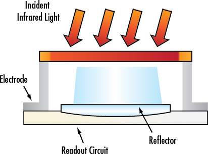
Figure 3: Illustration of Cross-Section of Microbolometer Sensor Array
Sensor Features
Pixels
When light from an image falls on a camera sensor, it is collected by a matrix of small potential wells called pixels. The image is divided into these small discrete pixels. The information from these photosites is collected, organized, and transferred to a monitor to be displayed. The pixels may be photodiodes or photocapacitors, for example, which generate a charge proportional to the amount of light incident on that discrete place of the sensor, spatially restricting and storing it. The ability of a pixel to convert an incident photon to charge is specified by its quantum efficiency. For example, if for ten incident photons, four photo-electrons are produced, then the quantum efficiency is 40%. Typical values of quantum efficiency for solid-state imagers are in the range of 30 - 60%. The quantum efficiency depends on wavelength and is not necessarily uniform over the response to light intensity. Spectral response curves often specify the quantum efficiency as a function of wavelength. For more information, see the section of this application note on Spectral Properties.
In digital cameras, pixels are typically square. Common pixel sizes are between 3 - 10μm. Although sensors are often specified simply by the number of pixels, the size is very important to imaging optics. Large pixels have, in general, high charge saturation capacities and high signal-to-noise ratios (SNRs). With small pixels, it becomes fairly easy to achieve high resolution for a fixed sensor size and magnification, although issues such as blooming become more severe and pixel crosstalk lowers the contrast at high spatial frequencies. A simple measure of sensor resolution is the number of pixels per millimeter.
Analog CCD cameras have rectangular pixels (larger in the vertical dimension). This is a result of a limited number of scanning lines in the signal standards (525 lines for NTSC, 625 lines for PAL) due to bandwidth limitations. Asymmetrical pixels yield higher horizontal resolution than vertical. Analog CCD cameras (with the same signal standard) usually have the same vertical resolution. For this reason, the imaging industry standard is to specify resolution in terms of horizontal resolution.
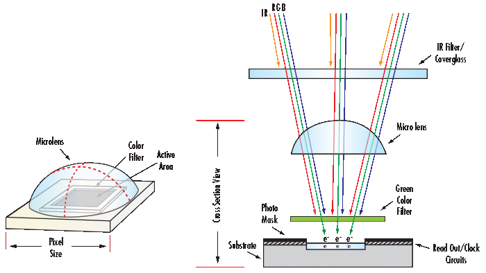
Figure 4: Illustration of Camera Sensor Pixels with RGB Color and Infrared Blocking Filters
Sensor Size
The size of a camera sensor's active area is important in determining the system's field of view (FOV). Given a fixed primary magnification (determined by the imaging lens), larger sensors yield greater FOVs. There are several standard area-scan sensor sizes: ¼", 1/3", ½", 1/1.8", 2/3", 1" and 1.2", with larger available (Figure 5). The nomenclature of these standards dates back to the Vidicon vacuum tubes used for television broadcast imagers, so it is important to note that the actual dimensions of the sensors differ. Note: There is no direct connection between the sensor size and its dimensions; it is purely a legacy convention. However, most of these standards maintain a 4:3 (Horizontal: Vertical) dimensional aspect ratio.

Figure 5: Illustration of Sensor Size Dimensions for Standard Camera Sensors
| Pixel Size (µm) | 9.9 | 7.4 | 5.86 | 5.5 | 4.54 | 3.69 | 3.45 | 2.2 | 1.67 |
| Resolution (lp/mm) | 50.5 | 67.6 | 85.3 | 90.9 | 110.1 | 135.5 | 144.9 | 227.3 | 299.4 |
| Typical 1⁄2" Sensor (MP) | 0.31 | 0.56 | 0.89 | 1.02 | 1.49 | 2.26 | 2.58 | 6.35 | 11.02 |
| Typical 2⁄3" Sensor (MP) | 0.59 | 1.06 | 1.69 | 1.92 | 2.82 | 4.27 | 4.88 | 12.00 | 20.83 |
Table 2: This table shows camera resolution by pixel size.
One issue that often arises in imaging applications is the ability of an imaging lens to support certain sensor sizes. If the sensor is too large for the lens design, the resulting image may appear to fade away and degrade towards the edges because of vignetting (extinction of rays which pass through the outer edges of the imaging lens). This is commonly referred to as the tunnel effect, since the edges of the field become dark. Smaller sensor sizes do not yield this vignetting issue.
Frame Rate and Shutter Speed
The frame rate refers to the number of full frames (which may consist of two fields) composed in a second. For example, an analog camera with a frame rate of 30 frames/second contains two 1/60 second fields. In high-speed applications, it is beneficial to choose a faster frame rate to acquire more images of the object as it moves through the FOV.
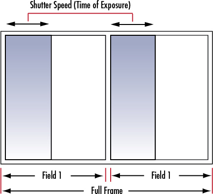
Figure 6: Relationship between Shutter Speed, Fields, and Full Frame for Interlaced Display
The shutter speed corresponds to the exposure time of the sensor. The exposure time controls the amount of incident light. Camera blooming (caused by over-exposure) can be controlled by decreasing illumination, or by increasing the shutter speed. Increasing the shutter speed can help in creating snap shots of a dynamic object which may only be sampled 30 times per second (live video).
Unlike analog cameras where, in most cases, the frame rate is dictated by the display, digital cameras allow for adjustable frame rates. The maximum frame rate for a system depends on the sensor readout speed, the data transfer rate of the interface including cabling, and the number of pixels (amount of data transferred per frame). In some cases, a camera may be run at a higher frame rate by reducing the resolution by binning pixels together or restricting the area of interest. This reduces the amount of data per frame, allowing for more frames to be transferred for a fixed transfer rate. To a good approximation, the exposure time is the inverse of the frame rate. However, there is a finite minimum time between exposures (on the order of hundreds of microseconds) due to the process of resetting pixels and reading out, although many cameras have the ability to readout a frame while exposing the next time (pipelining); this minimum time can often be found on the camera datasheet. For additional information on binning pixels and area of interest, view Imaging Electronics 101: Basics of Digital Camera Settings for Improved Imaging Results.
CMOS cameras have the potential for higher frame rates, as the process of reading out each pixel can be done more quickly than with the charge transfer in a CCD sensor’s shift register. For digital cameras, exposures can be made from tens of seconds to minutes, although the longest exposures are only possible with CCD cameras, which have lower dark currents and noise compared to CMOS. The noise intrinsic to CMOS imagers restricts their useful exposure to only seconds.
Electronic Shutter
Until a few years ago, CCD cameras used electronic or global shutters, and all CMOS cameras were restricted to rolling shutters. A global shutter is analogous to a mechanical shutter, in that all pixels are exposed and sampled simultaneously, with the readout then occurring sequentially; the photon acquisition starts and stops at the same time for all pixels. On the other hand, a rolling shutter exposes, samples, and reads out sequentially; it implies that each line of the image is sampled at a slightly different time. Intuitively, images of moving objects are distorted by a rolling shutter; this effect can be minimized with a triggered strobe placed at the point in time where the integration period of the lines overlaps. Note that this is not an issue at low speeds. Implementing global shutter for CMOS requires a more complicated architecture than the standard rolling shutter model, with an additional transistor and storage capacitor, which also allows for pipelining, or beginning exposure of the next frame during the readout of the previous frame. Since the availability of CMOS sensors with global shutters is steadily growing, both CCD and CMOS cameras are useful in high-speed motion applications.
In contrast to global and rolling shutters, an asynchronous shutter refers to the triggered exposure of the pixels. That is, the camera is ready to acquire an image, but it does not enable the pixels until after receiving an external triggering signal. This is opposed to a normal constant frame rate, which can be thought of as internal triggering of the shutter.

Figure 7a: Comparison of Motion Blur. Sensor Chip on a Fast-Moving Conveyer with Triggered Global Shutter (Left) and Continuous Global Shutter (Right)
Figure 7b: Comparison of Motion Blur in Global and Rolling Shutters. Sensor Chip on a Slow-Moving Conveyer with Global Shutter (Left) and Rolling Shutter (Right)
Sensor Taps
One way to increase the readout speed of a camera sensor is to use multiple taps on the sensor. This means that instead of all pixels being read out sequentially through a single output amplifier and ADC, the field is split and read to multiple outputs. This is commonly seen as a dual tap where the left and right halves of the field are readout separately. This effectively doubles the frame rate, and allows the image to be reconstructed easily by software. It is important to note that if the gain is not the same between the sensor taps, or if the ADCs have slightly different performance, as is usually the case, then a division occurs in the reconstructed image. The good news is that this can be calibrated out. Many large sensors which have more than a few million pixels use multiple sensor taps. This, for the most part, only applies to progressive scan digital cameras; otherwise, there will be display difficulties. The performance of a multiple tap sensor depends largely on the implementation of the internal camera hardware.
SPECTRAL PROPERTIES
Monochrome Cameras
CCD and CMOS sensors are sensitive to wavelengths from approximately 350 - 1050nm, although the range is usually given from 400 - 1000nm. This sensitivity is indicated by the sensor’s spectral response curve (Figure 8). Most high-quality cameras provide an infrared (IR) cut-off filter for imaging specifically in the visible spectrum. These filters are sometimes removable for near-IR imaging.
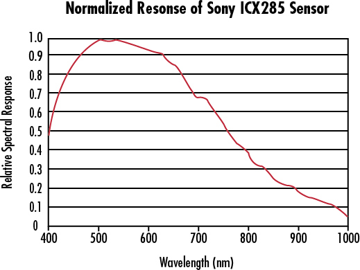
Figure 8: Normalized Spectral Response of a Typical Monochrome CCD
CMOS sensors are, in general, more sensitive to IR wavelengths than CCD sensors. This results from their increased active area depth. The penetration depth of a photon depends on its frequency, so deeper depths for a given active area thickness produces less photoelectrons and decreases quantum efficiency.
Color Cameras
The solid state sensor is based on a photoelectric effect and, as a result, cannot distinguish between colors. There are two types of color CCD cameras: single chip and three-chip. Single chip color CCD cameras offer a common, low-cost imaging solution and use a mosaic (e.g. Bayer) optical filter to separate incoming light into a series of colors. Each color is, then, directed to a different set of pixels (Figure 9a). The precise layout of the mosaic pattern varies between manufacturers. Since more pixels are required to recognize color, single chip color cameras inherently have lower resolution than their monochrome counterparts; the extent of this issue is dependent upon the manufacturer-specific color interpolation algorithm.
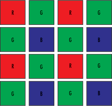
Figure 9a: Single-Chip Color CCD Camera Sensor using Mosaic Filter to Filter Colors
Three-chip color CCD cameras are designed to solve this resolution problem by using a prism to direct each section of the incident spectrum to a different chip (Figure 9b). More accurate color reproduction is possible, as each point in space of the object has separate RGB intensity values, rather than using an algorithm to determine the color. Three-chip cameras offer extremely high resolutions but have lower light sensitivities and can be costly. In general, special 3CCD lenses are required that are well corrected for color and compensate for the altered optical path and, in the case of C-mount, reduced clear ance for the rear lens protrusion. In the end, the choice of single chip or three-chip comes down to application requirements.
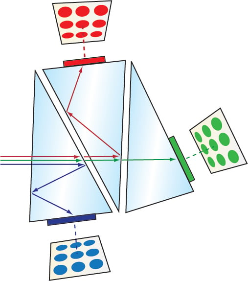
Figure 9b: Three-Chip Color CCD Camera Sensor using Prism to Disperse Colors
The most basic component of a camera system is the sensor. The type of technology and features greatly contributes to the overall image quality, therefore knowing how to interpret camera sensor specifications will ultimately lead to choosing the best imaging optics to pair with it. To learn more about imaging electronics, view our additional imaging electronics 101 series pertaining to camera resolution, camera types, and camera settings.


or view regional numbers
QUOTE TOOL
enter stock numbers to begin
Copyright 2025 | Edmund Optics BV, De Maas 22B, 5684 PL Best, The Netherlands
California Consumer Privacy Acts (CCPA): Do Not Sell or Share My Personal Information
California Transparency in Supply Chains Act
The FUTURE Depends On Optics®