Engineers are available to assist.

| Volume Pricing | |
|---|---|
| Qty 1-9 | €855,00 each |
| Qty 10-24 | €769,50 each |
| Need More? | Request Quote |
Edmund Optics offers comprehensive custom manufacturing services for optical and imaging components tailored to your specific application requirements. Whether in the prototyping phase or preparing for full-scale production, we provide flexible solutions to meet your needs. Our experienced engineers are here to assist—from concept to completion.
Our capabilities include:
Learn more about our custom manufacturing capabilities or submit an inquiry here.
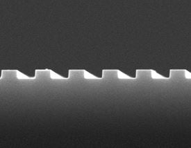
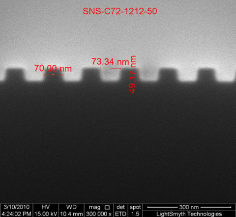
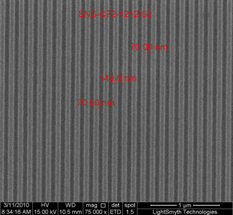
Coherent® LightSmyth™ Nanopattern Silicon Stamps consist of nanoscale-textured surfaces patterned on single-crystal silicon substrates. Through reactive ion etching, linear grooves with a trapezoidal cross-section are etched into the substrate surface, resembling conventional gratings. The etching process enables different period and depth specifications for these grooves, as well as more complex patterns such as lattices. Coherent® LightSmyth™ Nanopattern Silicon Stamps are ideal for nanophotonics research applications in the fields of optics and photonics, biology, chemistry, nanoimprinting, and microfluidics.
Note: II-VI Incorporated is now Coherent Corp.

These optics require special handling to avoid damage and ensure long-term performance. Proper handling, cleaning, and storage are essential to maintain optical quality. Explore our Optics Cleaning Resources for step-by-step guides and best practices. For personalized assistance, Email us or Chat with our technical support team.


or view regional numbers
QUOTE TOOL
enter stock numbers to begin
Copyright 2025 | Edmund Optics BV, De Maas 22B, 5684 PL Best, The Netherlands
California Consumer Privacy Acts (CCPA): Do Not Sell or Share My Personal Information
California Transparency in Supply Chains Act
This content may include material that has been generated or modified using artificial intelligence (AI).
The FUTURE Depends On Optics®